|
|
|
|
|

|
|
← Easy Chair CIA NRP SRT-91 →
The SP-program comprised a target element (TE), a suitable surveillance
receiver, a switch receiver and an activation transmitter.
Furthermore, it would be the first project in which new
micro-discrete (similar to SMD)
manufacturing facilities would be used for the target element.
It was the aim to make the target element much smaller than before,
whilst maintaining its low power consumption and superior
audio masking facilities.
In order to get acquainted with the new manufacturing technology,
it was decided to develop the new target element is several stages.
|
|
|
Unfortunately, the project did not progress as expected. There were several
set-backs when acquiring the new manufacturing equipment, building the new
cleanroom and setting up a new darkroom for photographic PCB production.
Furthermore, it took longer than anticipated to develop the required
skills for subminiature circuit production and to obtain the components.
Eventually, the development was
delayed for more than one year. Although several phases of development
were completed successfully, the final result was probably not what the
CIA had hoped for. Although this hasn't been confirmed yet, it seems likely
that the development was cancelled by the CIA in late 1973 or early 1974.
At the same time, the steady stream of research reports from the NRP came
to an end, indicating that this might have been the end of the open-end
Easy Chair research contract. After this point, no new
transmitters (bugs) were developed.
Nevertheless, production of existing bugs continued as before,
and several other products were developed for the CIA in the
following years, right until the demise of the NRP in 1993.
Furthermore, the lessons learned from the SP-project were used to improve
other products.
It is possible that the SP-bug was eventually built by a third party 1
in the US, as the SRT-99.
In 1979, the CIA briefly returned to the NRP for the reproduction of
the SRT-153 transmitter and its
peripherals.
|
 |
-
This has not been confirmed. It is known from later documents however,
that the SRT-99 was a similar transmitter, built by another contractor
and featuring the Dirty Pulse (DP) audio masking scheme
that had been developed by the NRP.
|
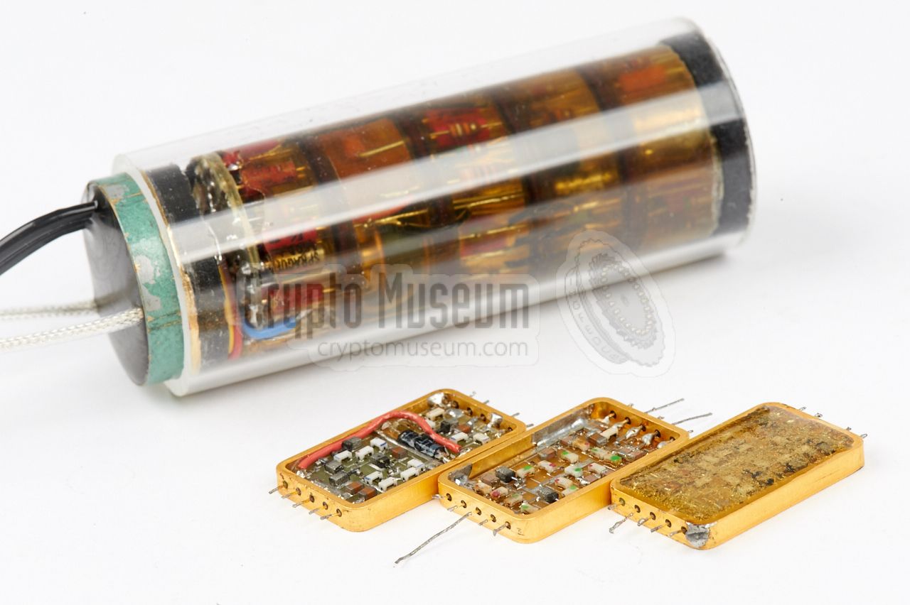
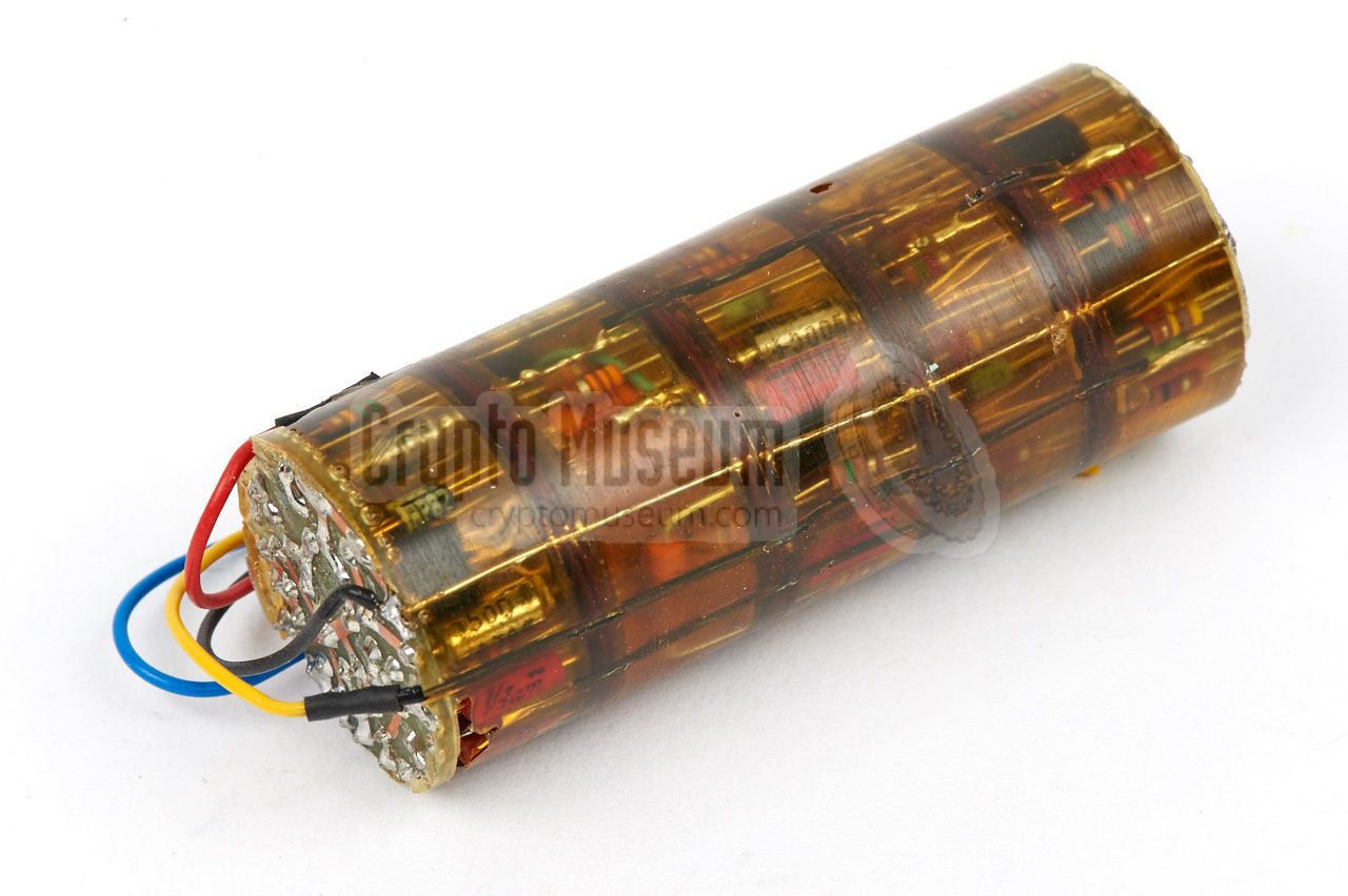
The diagram below shows a top view of the three modules in flat-pack enclosured, that form
the audio modulator. These were the first modules to be built with miniature
components. From left to right: the power regulator and the noise generator,
the video coder and the audio amplifier. Note that the first module houses
two separate circuit boards, plus a conventional zener diode.
|
|
A complete SP-SRS system consisted of the following parts:
|
|
Ever since covert listening devices (bugs)
were developed by the NRP,
the CIA kept asking for smaller units that would be easier to hide.
In the mid-1950s it had been the invention of the transistor that made
it possible to reduce the size and the power consumption dramatically.
|
In the mid-1960s the first integrated circuits (ICs) began to appear,
but these were hardly suitable for use in miniature transmitters.
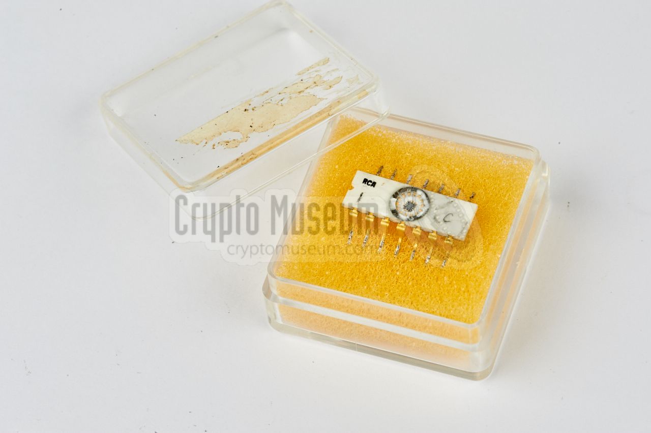
For military and other professional applications, developers sometimes
built sub-minature circuits onto a ceramic substrate, such as the
analogue IC shown in the image on the right.
In the example, unpackaged transistors are directly bonded to the substrate
and resistors are implemented as grey zig-zag lines.
Parts and packages for such miniature circuits were only available to
high-end customers at the time.
|
|
|
The CIA provided several examples
of these miniature circuits to the NRP,
in the hope that they would be able to use the technology in the design
of the next generation of transmitters. Other manufacturers had already
demonstrated their ability to shrink the size of a bug significantly.
The CIA even provided an
SRT-105 transmitter
as an example of another manufacturer's work.
Reducing the size of a pulse-based NRP transmitter was not a simple task though,
as it is much more complex than the average bug made by its competitors.
It contains an audio amplifier with a sophisticated compressor,
a video coder with advanced
audio masking techniques,
and a pulse-based RF unit that makes it almost impossible to find
with advanced TSCM sweeping techniques,
whereas the subcarrier (SC) modulated
SRT-105 can be
intercepted and located
within seconds.
|
To hide the RF carrier and its modulation from regular
surveillance receivers,
professional bugs often use a special technique
that is known as
audio masking.
The SP-TE uses a sophisticated masking scheme, based on Pulse Position
Modulation (PPM), known as
Dirty Pulse (DP) masking.
This masking scheme was also used in the
SRT-91 bug that had just
been developed. Initially, noise was added to the back porch of the
pulse, but test had revealed that reception of the signal in a
blocking receiver could lead to unwanted demodulation.
In the SP it was therefore decided to add the noise to the front
porch of the pulse. The SRT-91
was later modified for this as well.
This masking scheme is characterised by an AM carrier with a rather large
bandwidth (~ 7 MHz) and a multitude of sidebands at either side,
caused by the short square-wave pulses.
In addition, the front porch of each pulse is shifted in time, under
control of an internal random noise source.
There are currently no known commercially available
surveillance receivers
or bug tracers
that can readily demodulate a DP-masked
audio signal. Most receivers won't even lock onto the carrier.
➤ More about DP audio masking
|
Along with the SRT-91, a new modular receiver was introduced that was capable
of decoding the new Dirty Pulse (DP) masked audio signals.
It was known as SRR-91, and was just 6 cm high, so that it could easily be
fitted inside a standard executive style Samsonite briefcase of the era.
By installing the decoder module the other way around, the receiver could
also be used for decoding RP-masked bugs, such as the
SRT-56.
➤ More information
|
|
|
|
Signals from the SP-SRT can be received and demodulated with the following
receivers:
|
Detection and discovery of the bug is possible, but is not evident.
As far as we know, there are no commercially available
surveillance receivers that can readily
demodulate an DP-masked signal. Furthermore, existing bug tracers like the
Scanlock
do not lock onto its signal at all.
Finding and locating the bug is possible with a portable spectrum analyzer,
such as the
Rohde & Schwarz FSH-3,
and with a modern monitoring receiver like
the R&S PR-100 shown on the right.
➤ Read the full story
|
|
|
|
|
Micro-discrete manufacturing
LIDs
|
|
|
The later SRT-91
marked the move from circular cordwood structures to
small rectangular PCBs, using the smallest available components of the era.
Remember that these were the early 1970s, when surface mount devices (SMDs)
in consumer products were at least 10 years into the future.
Nevertheless, the SRT-91
was largely built with SMD parts, complemented
by conventional parts where necessary. These components were most likely
sourced from military supply chains, and were probably obtained with help
from the CIA,
as they were not commonly available at the time.
|
|
|
|
Despite the fact that the SRT-91
was smaller than its predecessors,
it was still too large to meet the CIA's requirements. Over the years,
the CIA constantly kept asking for smaller devices that were easier to hide.
Finally, in 1970, the NRP made a huge investment into new manufacturing
equipment for mounting super small electronic components directly onto
ceramic substrates.
|
At the time, the super small parts were known as leadless inverted
devices, or LIDs, comparable to the regular SMD parts of today.
The parts were directly bonded or glued to the wiring pattern of a
gold-plated ceramic substrate, similar to the first generation of
integrated circuits (ICs) [2]. 1
Mounting of the parts was done
under a microscope,
in a dust-free environment. Especially for this purpose,
the NRP had built a
cleanroom on the top floor of the building, complete with
the new manufacturing microscope and workstation
that is shown in action in the image on the right.
|
|
|
|
As the existing photographic reproduction equipment — used for making
printed circuit boards (PCBs) — was not accurate enough for the narrow
tracks on the substrate, that equipment had to be replaced as well.
The new darkroom was located adjacent to the cleanroom
on the top floor.
|
Around August 1971, the new equipment was delivered and
installed, and the NRP began experimenting with LIDs.
As this coincided with the development of the Super Pulse (SP) bug,
it was decided to build part of it in LID technology.
Resistors and capacitors were already available as LIDs, and to some
extent transistors as well. Tantalium capacitors came as bare
unpackaged parts in order to reduce their size somewhat.
Other parts had to be fitted externally as regular components.
The image on the right shows the first substrates made with the
new facilities.
|
|
|
|
The LIDs manufacturing technology was also used by other manufacturers
for making so-called hybrid or thick-film sub-circuits. In many cases
these hybrids were LIDs, mounted on a ceramic substrate that was then
cast in a strong protective epoxy. In military equipment, this technology
was often used to reduce size and weight, and to increase modularity
and service-friendlyness.
|
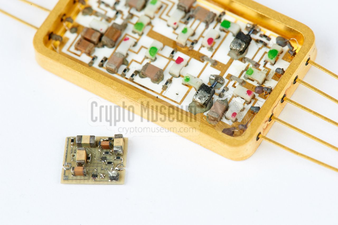
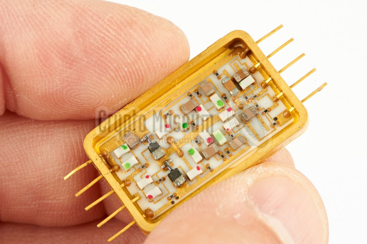
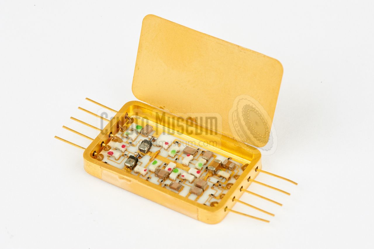
At the NRP, the substrates were mounted inside a gold-plated enclosure
with five leads at either side. Once the circuit was tested, the enclosure
was hermetically soldered by placing a gasket between the edge of the case
and the golden lid, and then heating it until the solder had melted.
As the technology was new, and the NRP still had to overcome several
hurdles — they were not yet able to miniaturise the RF module —
the video coder would be dealt with first. It comprised
3 modules: (1) regulator and noise generator,
(2) audio amplifier
and (3) the actual video coder.
|
|
|
|
Each module has five wire terminals at either side for connection to
the outside world. The three
modules of the video coder could be placed in-line — to make up one long
thin module — or on top of each other, in which case they were interconnected
by means of two small PCB planes.
|
Although the NRP went through great lengths to make the new LIDs manufacturing
technology successful, it is unclear whether they continued using it.
Experiments with thin
regular FR-4 PCB material
had meanwhile demonstrated
that it was just as suitable for minature manufacturing,
without the costly cleanroom requirements.
Apart from the parts described above, no other modules seem to have
been made in LID. From surviving documents it is known
that evaluation versions of the QRR switch receiver and the QRT actuator
were built and delivered to the CIA.
|
|
|
|
In late 1972, the stream of 6-monthly progress reports that had been flowing
to the CIA steadily since 1952, abruptly stopped. This might indicate that
the CIA had ended the Easy Chair research contract,
but it could also mean that they had simply changed their modus operandi.
In any case, the NRP continued to produce and service the existing
SRT-52,
SRT-56,
SRT-91
and SRT-107 bugs,
along with the matching receivers and several other products,
until its demise in 1993.
|
-
Leadless Inverted Devices (LIDs) were the predecessors of Surface Mount
Devices (SMDs). They were manufactured by
Philips subsidary
Amperex Electronic in New York (USA), who had earlier acquired
the technology by taking over Advanced Micro Electronics [2].
|
|
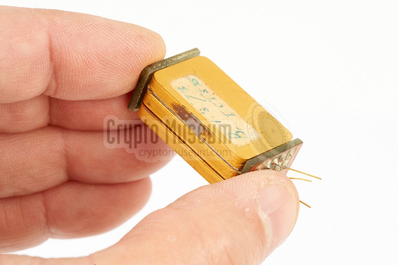
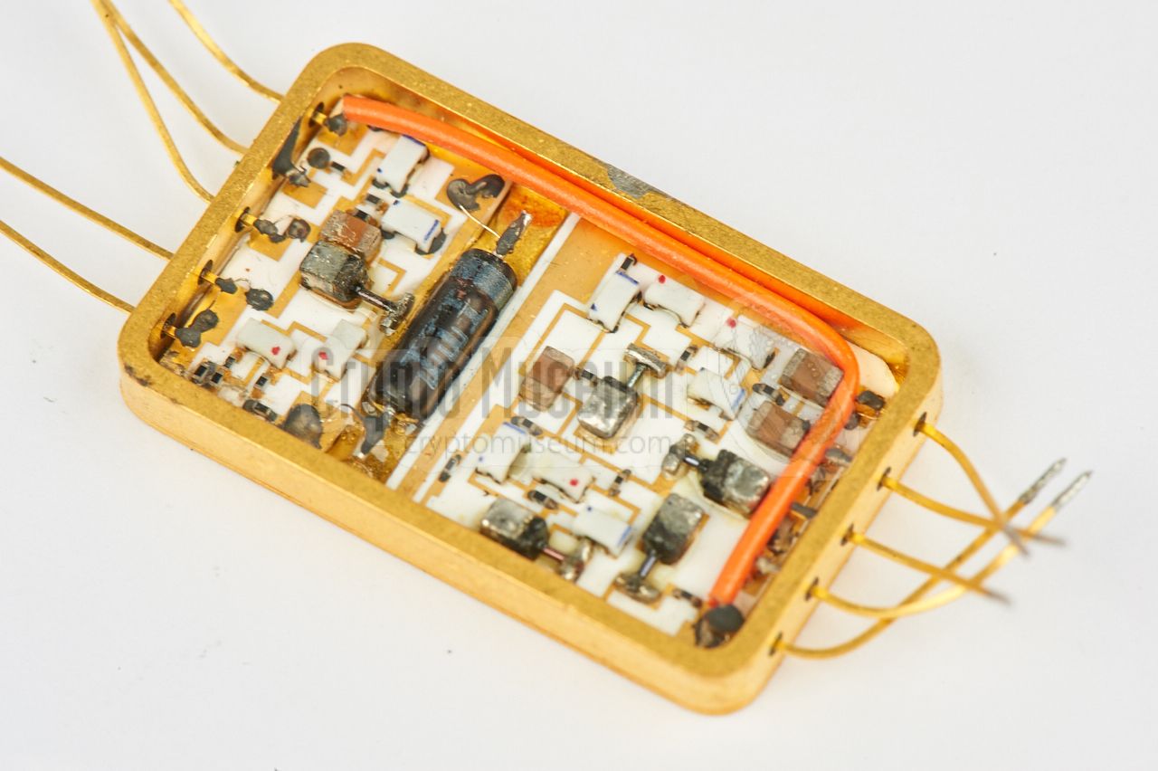
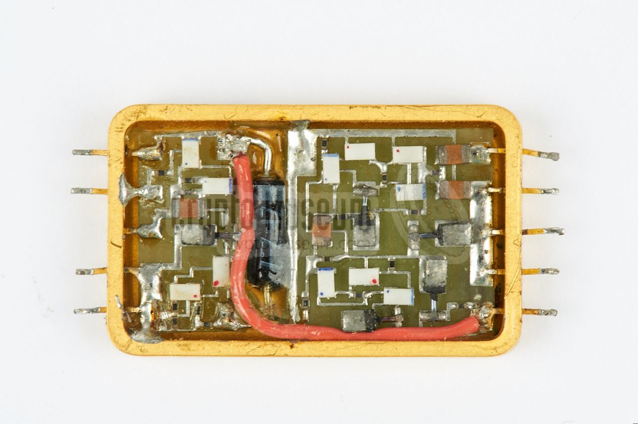
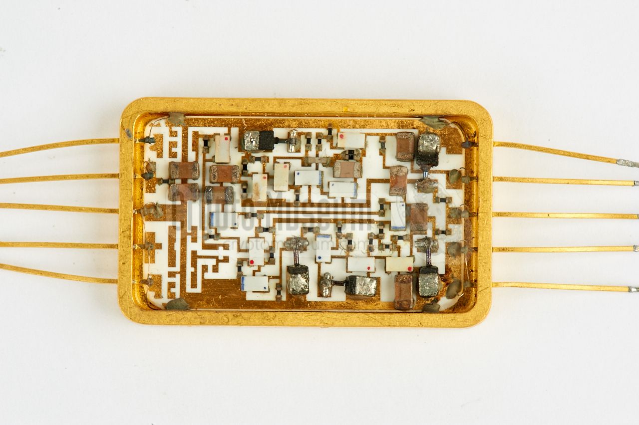
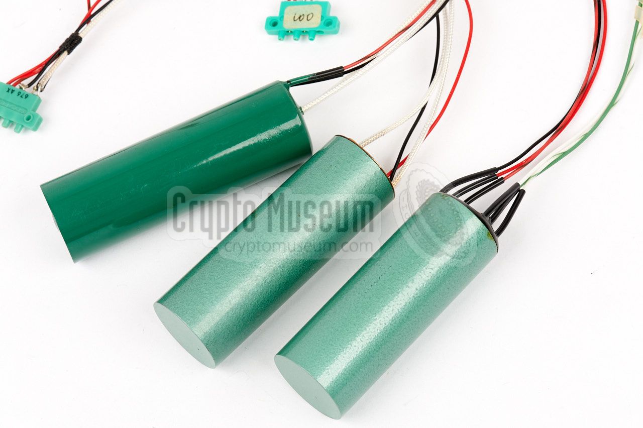
The modules are housed in identical flat-pack enclosures that measure
26 x 16 x 3 mm and have ten wire terminals (five at either side). It consists
of a machined cavity with rounded corners that is open at one side. After
manufacturing and testing, the open side is closed by soldering a gold-plated
lid over it. Once closed, it will be very difficult to open it again without causing damage.
|
|
|
Regulator and noise generator
|
|
|
The first unit contains two circuits, each of which is on a separate PCB.
The smaller PCB holds the power regulator. It is built around 4 transistors
and some passive components. A conventional zener diode is fitted in between
the boards. It wasn't available as a minature part at the time.
The larger PCB holds the noise generator that is used as part of the audio
masking scheme of the video coder. It is built around 7 transistors.
|
|
|
The amplifier is built around 13 - 16 transistors, depending
on the required features. It consists of a pre-amplifier, a main
amplifier, and an automatic level control (ALC) with detector.
In its full configuration, the amplifier has two microphone inputs
with muting capability. The image on the right shows a typical amplifier
of which the second microphone pre-amplifier and the muting circuit is
left off.
|
|
|
The video coder is at the heart of the modulator and is built around
15 transistors. It consists of a matrix, that mixes audio and noise,
a signal clock and a set/reset circuit for creating the output
pulses for the (external) RF-unit.
The noise is used to randomly change the position of the rising edge
of the pulse-modulated signal, rather than the trailing edge as in the
early version of the SRT-91. The SRT-91 was later modified to do the same,
along with the matching SRR-90 receiver.
|
|
|
|
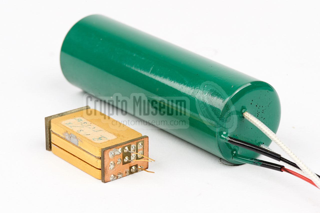
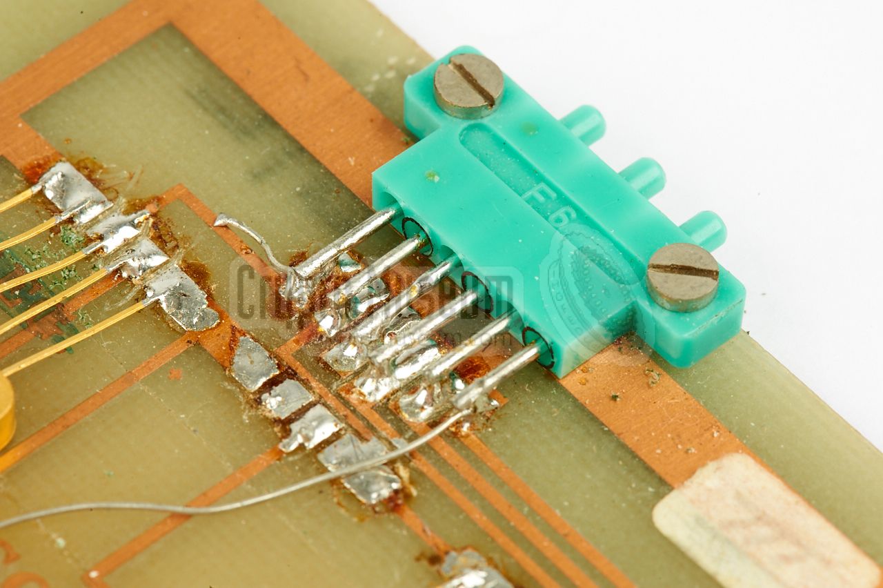
Once the modules were built, the wires were cut from the lead frame
and the three modules were temporarily soldered onto a single sided
PCB that acted as a test panel. The three modules were interconnected
via the PCB, ending in a 6-pin Socapex socket, similar to an SRT-56 video
coder.
|
The image on the right shows a test PCB, on which the regulator/noise
generator and the audio amplifier have been fitted. The space at the
centre is reserved for the video coder. It is bypassed here by a single wire
for testing.
The 6-pin Socapex connector is wired identically to that of the the existing
video coders of the earlier SRT-52 and SRT-56 transmitters, so that it can
be connected directly to an existing RF-unit for testing. Once the modules
had been tested successfully, the enclosures were solder-sealed and the modules
were ready for delivery.
|
|
|
It is likely that the modules were provided to the CIA on the test boards,
so that the CIA could quickly run an acceptance test before deployment.
The same procedure (with modules on a test board) was later used for
delivery of the SRT-153 transmitter
and the QRR-153 switch receiver.
|
The block diagram below illustrates the operation of the SRT-SP.
At the left are the three stacked PCBs, of which the bottom one contains
the microphone amplifier and the Automatic Gain Control (AGC).
The PCB in the middle contains the random noise generator and the power
regulator.
The upper PCB contains the actual video encoder, which is based on
a 20 kHz master oscillator and a flip-flop (FF), that is set by the
phase of the audio + noise signal, and reset by the phase of
just the audio signal. This results in a series of short pulses
with an average duration of 1µs, spaced 50 µs apart, that are used to
drive the keyer of the 340 MHz pulse transmitter at the right.
|
|
During the development of the Super Pulse (SP) modules, the meaning of the wire
terminals was changed several times. Furthermore, the power supply to
the units was at some point changed from negative (-V) to positive (+V),
which means that all NPN and PNP transistors had to be swapped. It is believed
that the diagrams below show the pinout of the final version.
|
|
| |
Regulator and noise generator
|
|
- Circuit diagrams of regulator, noise generator, amplifier and coder
NRP, 1970-1973. CM302711/A.
- Circuit diagrams of RF unit, switch receiver and activation transmitter
NRP, 1970-1973. CM302711/B.
- QRS-SP Evaluation Equipment
NRP, November 1972. CM302711/C.
|
|
|
|
Any links shown in red are currently unavailable.
If you like the information on this website, why not make a donation?
© Crypto Museum. Created: Tuesday 08 August 2017. Last changed: Sunday, 08 December 2019 - 11:23 CET.
|
|

|
|
|


![Manufacturing facilities at the NRP [2]](img/manuf.jpg)


